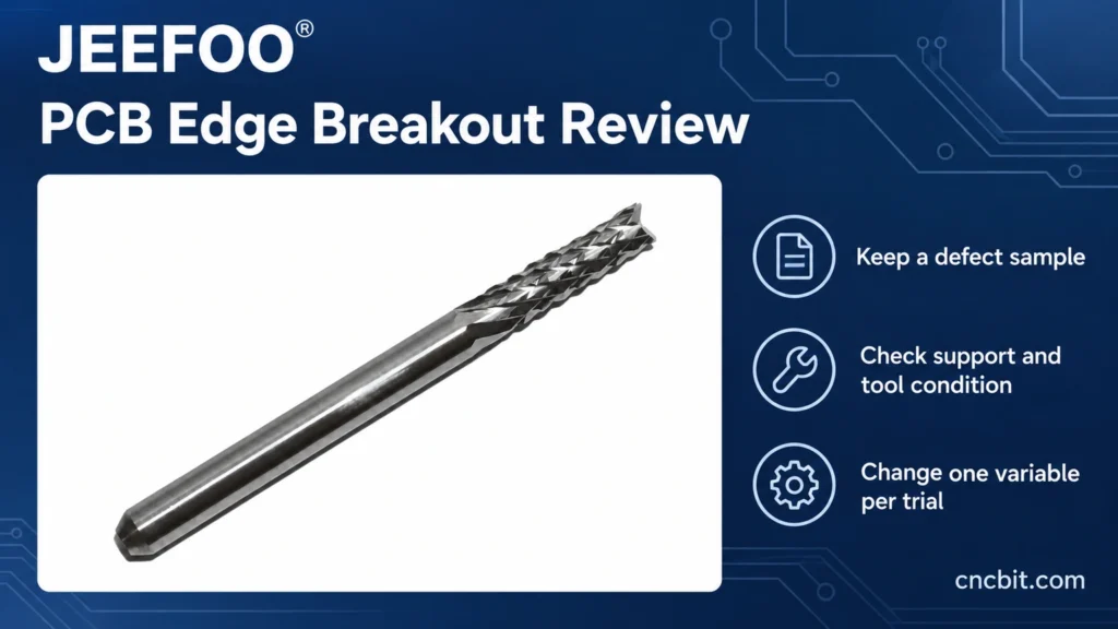
PCB edge breakout should be investigated by its location, appearance, and point of occurrence. Inspecting a damaged edge before changing settings helps distinguish machining damage from damage introduced when tabs are removed or boards are handled.
1. Preserve PCB Edge Breakout Evidence Before Rework
Set aside an affected board and photograph the defect with a scale and clear orientation. Mark the top face, bottom face, machining direction if known, and nearby features. Note whether material is missing, fibres project from the edge, copper is raised, or layers appear separated. These observations describe different conditions and should not be combined into a single vague finish complaint. Avoid polishing away the evidence before the cause has been reviewed.
2. Map When and Where the Damage Appears
Compare boards before and after depaneling or manual handling. Record whether the problem follows a particular corner, a tab, one side of a stack, or a specific fixture location. Look at earlier accepted parts from the same job when available. A simple annotated outline can reveal a repeating location more clearly than a collection of unlabelled photographs. Record the production stage at which each sample was inspected.
3. Review the Cutting Setup Systematically
Check tool identity and visible condition, board restraint, and any gaps in a stacked setup. Review spindle and holder condition using the machine maker’s procedures. UNION TOOL’s router troubleshooting guidance identifies wear, unstable boards, and runout among factors associated with poor edges. These are useful investigation categories, not proof of the cause on a particular machine. Do not assume that increasing spindle speed or reducing feed will resolve every defect.
4. Run a Controlled Comparison
Choose one justified change and document it before the next trial. Keep material, inspection lighting, magnification, and acceptance criteria consistent. Compare both edge appearance and critical dimensions, since a cosmetically improved edge can still miss the drawing. If discussing the trial with JEEFOO®, provide the PCB tool reference, laminate details, defect photographs, and the conditions before and after the change. Stop the trial if damage worsens or the setup becomes unstable. Use the same sample labels in photographs, measurement results, and trial notes so comparisons remain traceable.
An effective PCB edge breakout review links a visible defect to a specific stage and location. Preserve samples, investigate the setup, and accept changes only after the finished board meets the agreed requirements.
PCB Edge Breakout: Quick Answers
Does a damaged edge prove the router bit is worn?
No. Tool condition is one investigation category. Board movement, gaps in a stack, spindle runout, tab removal, and handling also need review. Record when the damage first appears before assigning a cause.
What should defect photographs show?
Include a scale, board orientation, top and bottom faces, and the defect location. Describe missing material, projecting fibres, raised copper, or apparent layer separation separately. Preserve an affected sample before rework.
Should feed or spindle speed be changed first?
There is no universal first adjustment. Inspect the tool, restraint, stack, holder, and machine condition, then select one justified change. Compare labelled samples under consistent inspection conditions and verify critical dimensions.
What information helps a tooling enquiry?
Provide the PCB tool reference, laminate details, defect photographs, stack and fixture arrangement, and the settings before and after the trial. Include the production stage and board location so the comparison remains traceable.